
NEXTECK SINGAPORE PTE LTD

ELEGRIP TAPE
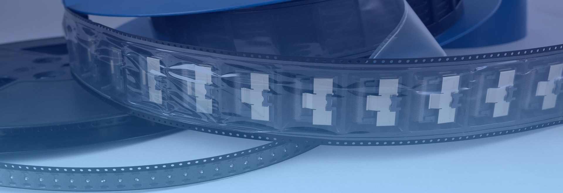
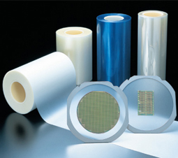
COVER TAPE
ALS, ATA, MT8, TIST 100, 300 grade, Highly transparency
Cover tape film with excellent sealing performance
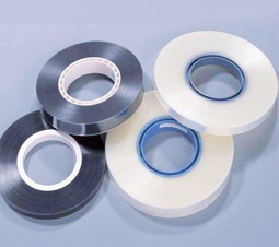
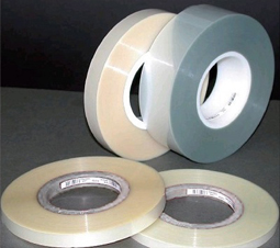
Dicing Tape,fixing semicon, silicon, GaAs during dicing
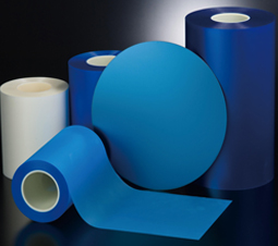
Back Grinding Tape,protect circuit surface during back grinding
© Copyright 2019-2024 NEXTECK. All rights reserved | Design by NEXTECK.COM