WLCSP Package Guide & Shipping Options
(1)
(WLCSP) Wafer-level chip-scale packages are an advanced package style in which the semiconductor integrated circuit (IC) is mounted directly to the (PCB) printed circuit board face-down, by way of solder balls that are attached directly to the IC without the need for an interposer or wire-bonds. This enables the use of a smaller solder ball diameter and tighter ball pitch, as well as a shorter electrical path between the IC and PCB, resulting in improved electrical and thermal performance, as well as reduced package assembly requirements.
(2)
Nexteck R&D team recommended WLCSP Shipping solution and options.
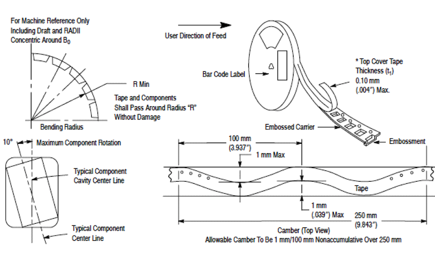
WLCSP devices are offered mainly in 13” Reel- and- Tape (R&T) shipping configurations. typical segment of embossed carrier tape, including the pockets where the individual WLCSP devices would be placed and the sprocket holes for feeding the tape into automated assembly equipment. The devices are placed with the solder balls facing down and pin 1 orientation for all devices in the same location. Adhesive cover tape is used to seal the devices in their pockets.
(3)
Nexteck Singapore Pte ltd, offers the full package of materials and solutions for the packaging and shipping of WLCSP on perfect matched Precision Carrier tapes and Embossed Cover tape to ensure the safety on logistic and peeling smoothness on finial process to PCBs and devices.