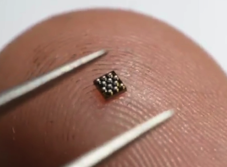
Wafer Level Chip Scale Package (WLCSP)
Wafer Level Chip Scale Package (WLCSP) refers to the technology of packaging an integrated circuit at the wafer level, instead of the traditional process of assembling individual units in packages after dicing (dicing tape is supplied by www.nexteck.com.sg) from a wafer.
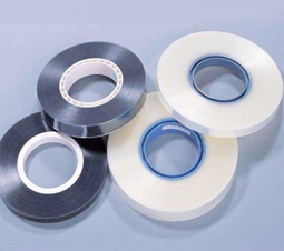
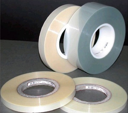
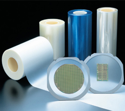
This process is an extension of the wafer Fab processes, where the device interconnects and protection are accomplished using the traditional fab processes and tools. In the final form, the device is a die with an array pattern of bumps or solder balls attached at an I/O pitch that is compatible with traditional circuit board assembly processes. WLCSP is a true chip-scale packaging (CSP) technology, since the resulting package is of the same size of the die. WLCSP normally at 01005 (inches) which need special packing materials like special designed carrier and cover tape supplied by Nexteck Singapore Pte Ltd.
Any further inquiry for dicing tape and packing materials (like carrier tape & cover tape) for WLCSP, please feel free to contact info@nexteck.com.sg or visit www.nexteck.com.sg.