WAFER LEVEL CHIP SCALE PACKAGE (WLCSP) & PACKING
 WLCSP solutions provide significant package footprint reductions, lower cost, improved electrical performance, and a relatively simpler construction over conventional wire-bond or interposer packaging.
What is the advantage of WLCSP ?
WLCSP is the smallest possible package size since the final package is no larger than the required circuit area. All of the manufacturing process steps are performed in parallel at the silicon wafer level rather than sequentially on individual chips to achieve a package that is essentially the same size as the die. The resultant package has dielectrics, thin film metals, and solder bumps directly on the surface of the die with no additional packaging. The basic structure of the WLCSP has an active surface with polymer coatings and bumps with bare silicon exposed on the remaining sides and back of the die.
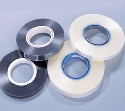
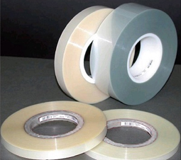
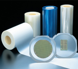
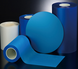
Nexteck Singapore Pte Ltd., Packing solution of WLCSP devices:
Tape-and-Reel is packed for transportation and storage. Packing media are designed to protect devices from electrical, mechanical and chemical damages (as well as moisture absorption).
Nexteck Group, the leading WLCSP packaging materials supplier in Singapore, Malaysia, Thailand and the Philippines, straighty enforce in proper handling and storage, protect from dropping packs, storage within 40 °C/90 % environment. Nexteck Singapore Pte Ltd. Our WLCSP Tape-and-Reel, complies with EIA-481B and EIA-481C and complies to orientation of devices with EIA-481D.